
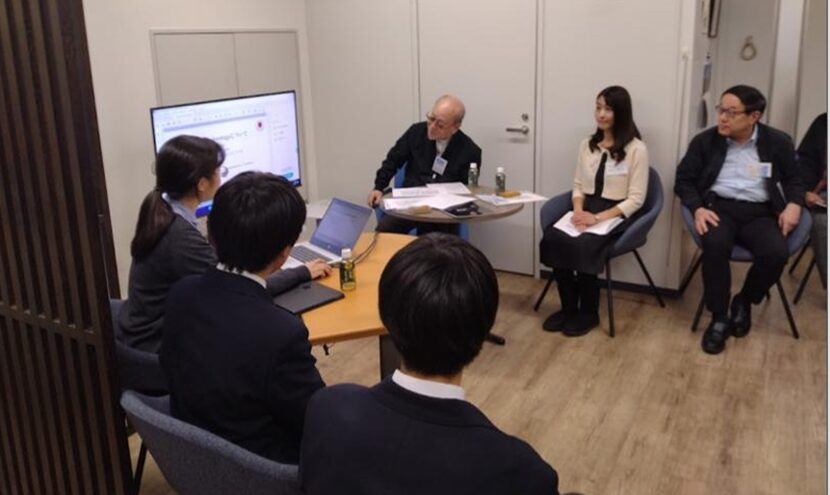
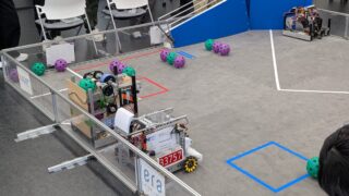
The other day, I visited the office of HIT INTERNATIONAL in Kofune-cho, Nihonbashi. First, from Yabusame Technology, we explained the activities of the FRC tournament and the team, and gave advice on the activities of Yabusame Technology from Hit International employees. After that, I had a lot of interesting talks about the company.
In this blog, we will report on the state of the visit!
About Hit International
Hit International Co., Ltd. is a company that mainly manufactures the parts necessary for manufacturing semiconductors.
We have developed products related to semiconductors, such as the development of a device for polishing silicon wafers, which can be used as a base for semiconductor integrated circuits (ICs), and the machine 'direction shape measuring machine' that manages the shape of the plate.
It is sold not only in Japan but also in various regions such as North America, Europe, and Asia.
In addition to semiconductor manufacturing, we are developing a technology called 'Lastrestor' that prevents rust from rusting of automobiles.
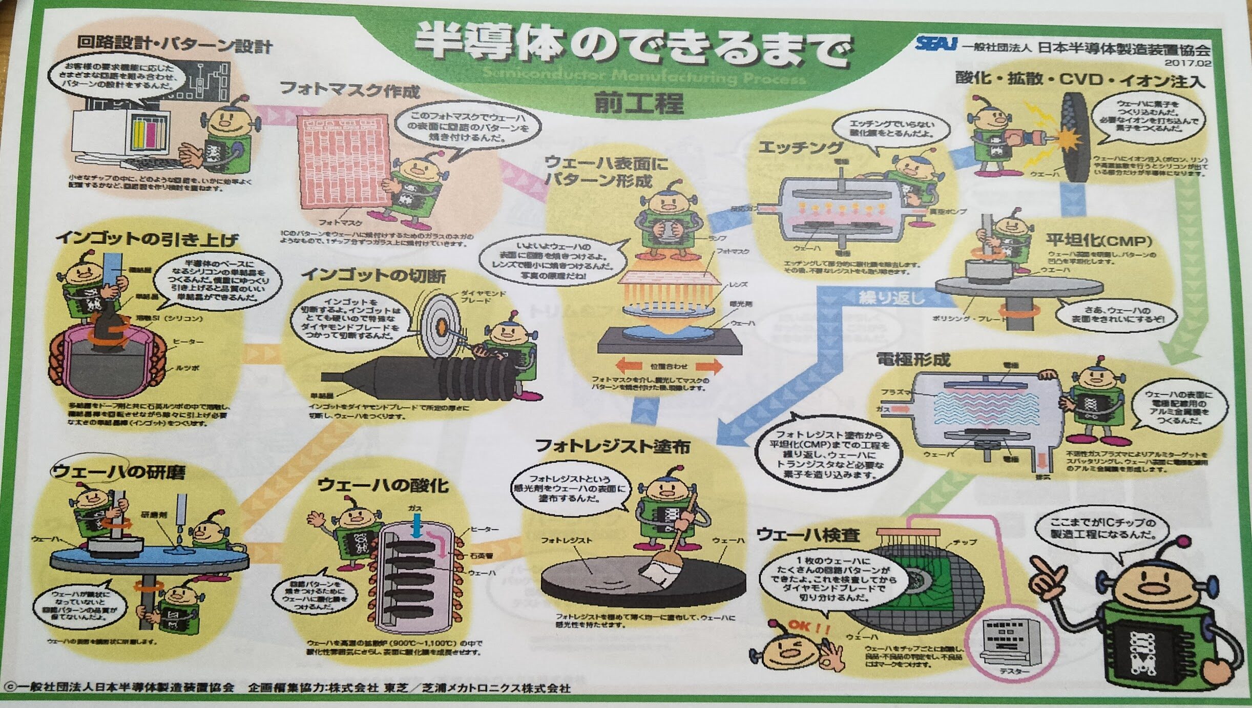
Semiconductor manufacturing
Semiconductor manufacturing is mainly divided into a pre-process and a post-process.
The first step is the pre-process.
Silicon wafers, which can also be called the heart of a semiconductor, are made of a thin disk-shaped base made of silicon single crystal, and an IC is built on top of it. It is completed by slicing and polishing silicon by slicing and polishing the silicon from the silica stone, which is the raw material. In this case, the 'wrapping plate' is used.
After that, a thin film layer that becomes wiring or transistors is formed on the wafer and a photoresist (photosensitive material) is applied. Then transfer the circuit pattern on the photomask (like the 'type' that creates a fine circuit). After the transfer, the thin film is processed into the shape of wiring or the like in a process called edging.
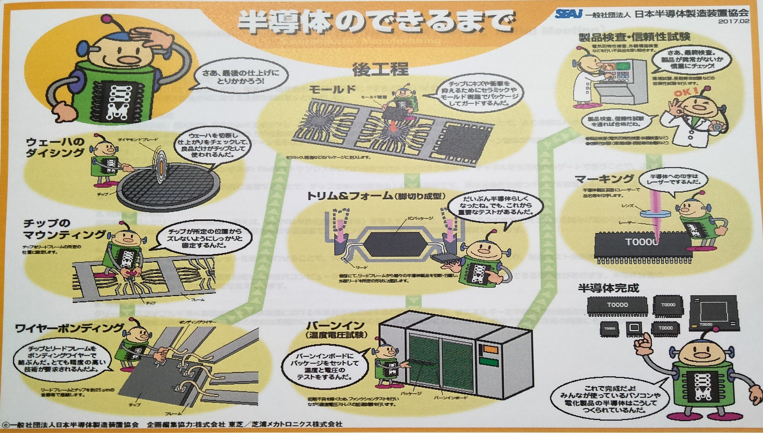
In the post-process, the wafers made in the pre-process are cut off and the chips essential for semiconductors are cut off. Then, the semiconductor is completed by fixing and enclosing the chip in place.
In this way, you can see that the process of manufacturing the silicon wafer, which is the base of the chip, is very important.
In addition, in the latest semiconductor manufacturing, technology that uses 'extreme ultraviolet' and technology for large-scale systems such as 'chiplet technology' is used.
visit
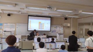
After hearing the explanation about the semiconductor manufacturing process, we were shown what was actually used in the manufacturing process.
Below we introduce them one by one!
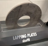
①Wrapping plate
It is a disc with a pattern of lattice that is precisely separated one by one. When you think of semiconductor manufacturing, you think of a small amount of work, but the wrapping plate is said to have a radius of about 2m. The sample I actually saw is part of it, but I was surprised at the scale of semiconductor manufacturing.
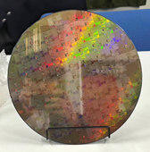
(2) Silicon wafer
As you can see in the image, the finished silicon wafer had a polished surface and was reflected like a mirror.
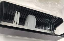
(3) Polishing carrier
It is used to fix the wafer when polishing. I was surprised by the unexpected way of using it, which is hard to imagine from the appearance.

④ Substrate
Although the substrate is a little different from semiconductor manufacturing, it is a disc-shaped piece made of glass in a hard disk such as a personal computer. This is where it's called 'hard disk'. The surface was shiny and very beautiful.
It was very interesting to be able to see things that you can't usually see! I felt a sense of familiarity with semiconductor manufacturing!
This time, I was able to listen to not only about semiconductor manufacturing, but also what I should be aware of when developing overseas business. He gave me advice on the importance of building trusting relationships with friends from abroad and avoiding credit risk.
After the exchange meeting, we had dinner together with the members. During the meal, in addition to advice and technical information exchange regarding robot production, I was able to hear various helpful stories such as the experiences of countries such as the United States, Saudi Arabia, Iran, and Russia, and it was a pleasant memory.
Thank you very much to all of Hit International for treating us with a variety of hospitality and dinner!
It's less than a month away from the performance. We will do our best to make it our goal for the world competition!
No responses yet